Overview
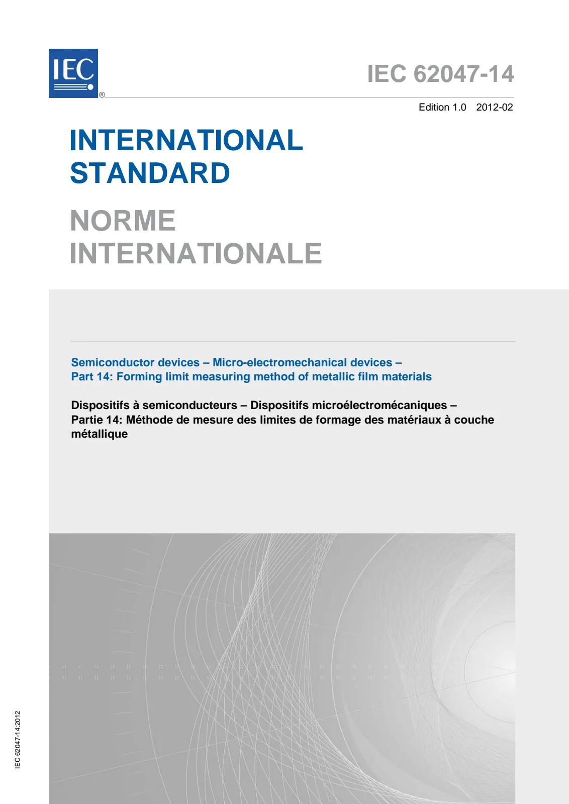
IEC 62047-14:2012 is an international standard published by the International Electrotechnical Commission (IEC) focusing on semiconductor devices-specifically micro-electromechanical systems (MEMS). This part 14 standard details the forming limit measuring method for metallic film materials with thicknesses ranging from 0.5 µm to 300 µm. These metallic films are integral to electric components, MEMS, and other micro-devices.
The standard provides a comprehensive method to predict material failure during forming processes, such as imprinting, which is critical for improving the reliability of MEMS components. By applying this standard, manufacturers can reduce product development time and lower manufacturing costs while enhancing component quality and durability.
Key Topics
-
Scope and Application
Defines procedures and terminology related to measuring the forming limits of metallic films used in MEMS and semiconductor devices.
-
Terms and Definitions
Includes specific terminology such as circular grids, square grids, major and minor axes of deformation, and strain symbols used in forming limit analysis.
-
Testing Methodology
Describes the forming limit diagram (FLD) measurement using a hemispherical punch that applies pressure to metallic films until fracture. It highlights the use of high-resolution digital imaging for accurate strain measurement.
-
Equipment Requirements
Specifies micro press equipment with a hemispherical punch, recommending hard chrome coating and lubricants like graphite to minimize surface friction. It also sets standards for punch speed (under 20 µm/s) to reduce dynamic effects during testing.
-
Specimen Description
Details the rectangular shape and varying aspect ratios of specimens tested to generate a comprehensive FLD-six aspect ratios (1.0 to 7.0) are recommended.
-
Data Analysis and Reporting
Provides guidelines on analyzing strain data to plot forming limit diagrams that predict failure locations in metallic films. The standard guides proper documentation of test results.
-
Supporting Annexes
Includes informative annexes covering principles of FLD, grid marking methods (photographic and inkjet), specimen gripping techniques, and strain measuring using digital camera-based image analysis.
Applications
-
MEMS Manufacturing
Enables designers and manufacturers to predict forming failures during imprinting and other forming processes, improving MEMS device reliability and product lifecycle.
-
Material Science and Engineering
Supports the characterization of metallic films to optimize materials used in semiconductor devices, leading to better formability and durability.
-
Quality Control in Semiconductor Production
Utilized for quality assurance to verify forming limits and prevent premature material failure during micro-device fabrication.
-
R&D for Micro-Devices
Aids in fast-tracking development cycles by providing accurate forming limit data, reducing trial-and-error phases and lowering development costs.
-
Process Optimization
Helps in selecting suitable film thicknesses and forming process parameters to maximize manufacturing yield and device performance.
Related Standards
-
IEC 62047-1:2005 - Semiconductor devices – Micro-electromechanical devices – Part 1: Terms and definitions; foundational for terminology used in IEC 62047-14.
-
General IEC Semiconductor Device Standards - Other parts of the IEC 62047 series address micro-electromechanical system components, providing a broad framework for standardized testing and design.
-
ISO/IEC Directives, Part 2 - Governs the drafting process for IEC standards, ensuring consistency and international consensus.
Keywords
IEC 62047-14, forming limit measurement, metallic film materials, MEMS reliability, micro-electromechanical devices, micro press equipment, forming limit diagram, strain measurement, semiconductor manufacturing standards, imprinting process failure prediction, micro-device material testing, micro-fabrication standards.

 Open preview (PDF)Semiconductor devices - Micro-electromechanical devices - Part 14: Forming limit measuring method of metallic film materials